The traditional XRD method uses monochromatic X-ray beam with energy insensitive detectors resulting in large and slow apparatus. The spectral sensitivity of every pixel in AdvaPIX TPX3 camera with high resolution Timepix3 chip enables polychromatic X-ray beam to be used for XRD (called Energ Disperdive XRD = EDXRD) resulting in much faster and more compact system:
- A polychromatic X-ray beam is easy to get directly from a common X-ray tube reaching high intensity => system is faster, smaller, much less complex.
- The high resolution detector can be placed close to the sample covering a large solid angle => mechanical angular scanning is not needed => fast data accumulation.
- Broad energy range (3 – 150 keV): Even very absorbing samples can be analyzed (stainless steel, heavy metals and minerals).
A combination of all these benefits brings acceleration by two orders of magnitude.
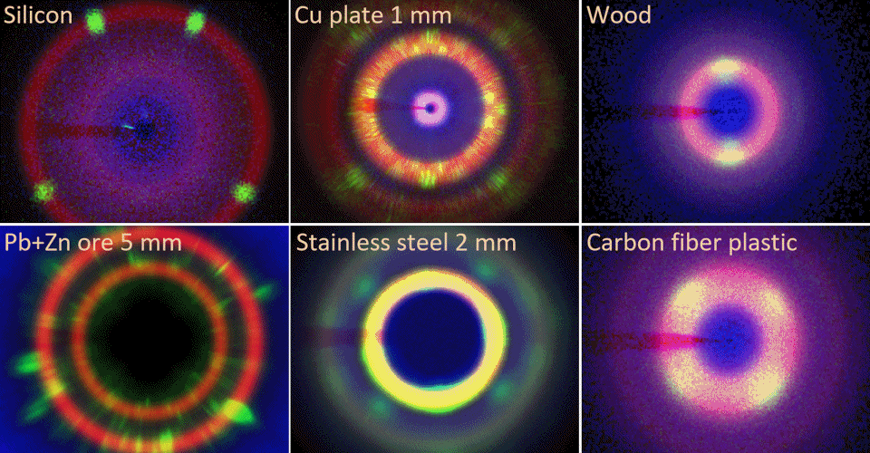
Examples
Several illustrative measurements are shown in the image below. The measurements performed in transmission mode (X-ray beam penetrates through the sample, detector is placed behind of it) with polychromatic X-ray beam of 80 kVp (or 160 kVp for metallic samples shown in the middle) collimated to 0.5 x 0.5 mm, sample to detector distance of 25 mm. The last column of organic samples (wood, carbon fibers plastic) shows anisotropic scattering patterns instead of XRD patterns. Measured in DTU laboratory by Jan Kehres (DTU) and Jan Jakubek (ADVACAM).

Color coding in these images shows powder signal in red, reflections from larger crystals in green and mean energy in blue.
Recrystallization due to annealing
Example of annealing due to spot welding of two 1 mm thick sheets of stainless steel is shown below. The texture of grain orientation caused by rolling is gradually annealed out in proximity to the weld area. The texture is presented as four bright spots between two rings close to the image diagonals in frame 1). These spots are gradually stretched in frame 2) till they cover whole circle in frame 3) indicating that directional organization of grains is getting more and more isotropic due to annealing.

It is important to remind that this measurement is showing material properties in its whole volume not only at the surface as often done by standard XRD.
This measurement was performed with X-ray beam of 160 kVp to get good signal through 2 mm of stainless steel. Result is shown after transformation to 50 keV.
XRD of 5 mm thick lead ore – is it possible?
The traditional XRD method in transmission geometry is difficult to be used for highly absorbing materials since it is very difficult to create monochromatic X-rays with energy high enough to penetrate them. The only way would be usage of large synchrotron sources.
Here we show the X-ray diffraction pattern for 5 mm thick lead ore with Pb content of 30% measured with a standard X-ray tube. The measurement was performed at 160 kVp. The image shows two selected energy channels: the first represents the maximum of the transmitted spectrum below the K absorption edge of lead at 70 keV and the second shows maximum above the K-edge at 120 keV. The diffraction rings are seen clearly for both energies. The transmission spectrum is shown as well (green line).

How does it work?
A basic principle of the “Energy Dispersive X-ray Diffraction” (#EDXRD) with our spectral imaging detector is described in the following animation. It illustrates powder diffraction in transmission geometry.

Instead of taking single diffraction image accumulating all X-ray energies (wavelengths) into single image as performed in traditional XRD apparatus, we record about 150 images – one for each energy channel (usually 1 keV wide). Then using Bragg formula we transform (stretch or shrink) each of these particular images to fit one selected energy (e.g. 40 keV) and then we sum all of them getting single final image with high statistics. This way all primary energies contribute to the image instead of being lost in monochromator. The measurement is therefore significantly faster.
The transformation (shrinking) of each individual image for particular energy channel to one selected energy is shown in next animation for silicon powder sample.

The X-ray beam size was 0.5 x 0.5 mm and the sample thickness was about 1 mm. The spectral images in interval from 20 to 40 keV are used. The energy channel image (left) is recalculated to 40 keV (right) and then all off them are summed up.
 The following example of diffraction in single crystal of Silicon wafer is even more illustrative.
It shows individual spectral images transformed to 40 keV. Then it shows circular integration, energy spectra for all reflections and determination of lattice constant d (measured as 54 pm).
Choice of sensor material
The #Timepix3 detector sensitivity is defined by its sensor chip material and thickness. Generally speaking: The thinner silicon sensors provide better energy resolution, while thicker or #CdTe and #CZT sensors provide better sensitivity for high X-ray energies. Next picture shows comparison of several sensor types for XRD of a silicon powder.

The influence of energy range and energy resolution for different sensors can be illustrated by following maps:

The horizontal axis is energy [E], vertical axis is ring radius [r]. Each point [E,r] in this map has intensity calculated from measured spectral image for energy E as integral along the ring with radius r. So, for the ideal sensor there should be narrow lines spreading over the whole X axis and signal out of these lines would be zero. Narrow lines express fine energy resolution (narrower better), signal out of lines represents the background (smaller better) and the length of lines along X axis shows the energy range (longer is better).
The thin Si sensor (left most image) has the best energy resolution (thin lines) but narrowest energy range (short lines). The 2 mm thick CdTe and CZT sensors provide broadest energy range (lines stretch over the whole X axis) but much worse energy resolution (broad lines).
Angular resolution
The XRD resolving power (angular resolution) of the described system depends on three factors: a) Pencil beam size, b) sample thickness, c) detector energy resolution. In all presented pictures of this article the two first factors dominate.
The influence of energy resolution to angular resolution depends on lattice constant d and energy. Generally speaking: higher energy better angular resolution and smaller lattice constant worse angular resolution. For instance angular resolution achieved with thin Silicon sensor for silicon crystal sample at energy of 40 keV is 0.5 deg rms (3.1%), while at 60 keV it is 0.28 deg rms (2.5%). For iron sample at energy of 40 keV the resolution is 1.16 deg rms (3.4%), while at 60 keV it is 0.56 deg (2.6%). It is important to note that detection efficiency of Silicon sensor at 60 keV is already very low.
X-ray diffraction in general
The X-ray diffraction technique is used for inspection of crystalline structure of samples on macro- or microscopic level. It provides information on crystal types (phase), crystallization level, granularity, grain orientation or texture. All these phenomena affect mechanical material properties such as hardness, fragility, ductility, abrasivity or abrasion resistance. The #XRD can be used also for internal strain mapping especially after special technological steps such as welding, surface hardening or annealing. The #XRD method is often used as analytical method in mineralogy and mining.
Are you curious about how our technology can improve your field?